2nm Manufacturing Costs to Double Those of 4nm and 5nm, Posing Challenges for the Industry
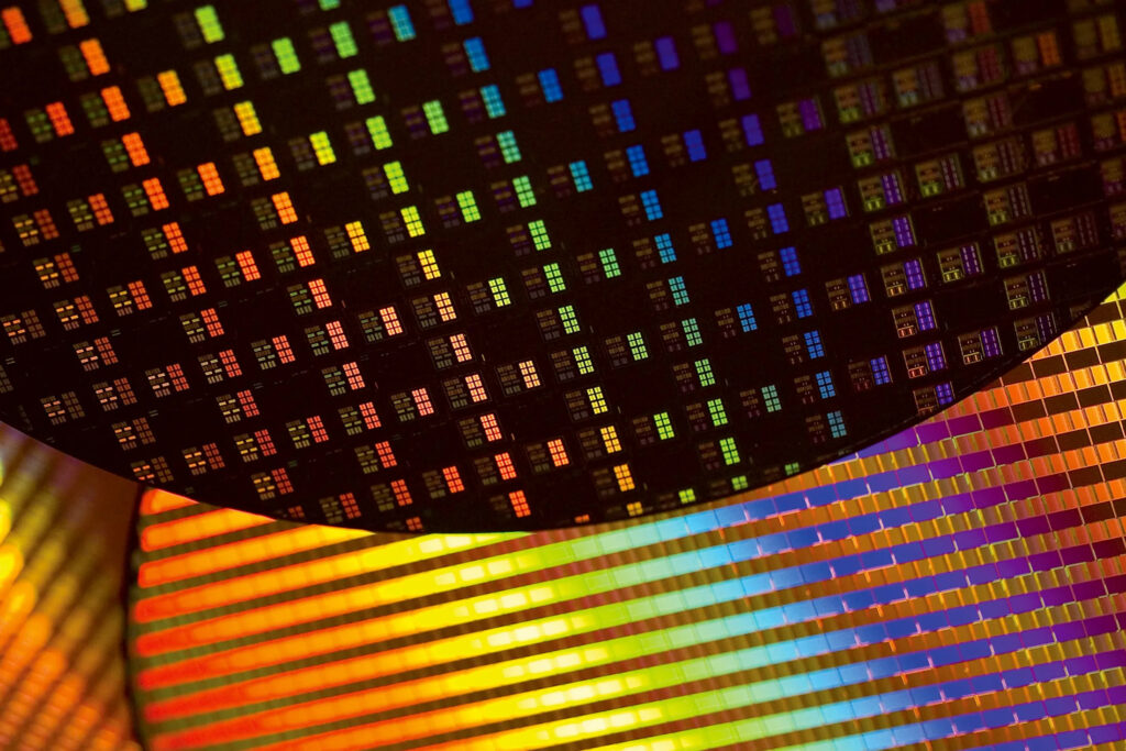
TSMC’s new N2 (2nm-class) manufacturing process is poised to offer significant advantages, including the introduction of nanosheet gate-all-around transistors and NanoFlex technology. However, it comes with a steep price tag. According to reports from the China Times, the price for a 300-mm wafer processed using N2 technology will exceed $30,000. This represents a significant increase from the $15,000 price of an N4/N5 wafer and even surpasses the earlier estimates of $25,000 for N2 wafers.
While TSMC’s pricing can vary depending on customer and volume, this projected increase highlights the cost-intensive nature of the N2 process. For comparison, N3 (3nm-class) wafers currently cost around $18,500. The price surge for N2 technology is linked to the inclusion of advanced production techniques like nanosheet transistors and the high cost of extreme ultraviolet (EUV) lithography equipment, each costing about $200 million.
Despite the high price, TSMC’s N2 process promises significant improvements in performance, power efficiency, and transistor density. Chips produced using the N2 process are expected to deliver 10% to 15% better performance at the same power, while power consumption could be reduced by 25% to 30%. Additionally, transistor density is projected to increase by approximately 15%, offering more processing power in a smaller area.
N2 technology will also give designers greater flexibility by allowing them to fine-tune performance and power efficiency through adjustments to the width of transistors. Moreover, the NanoFlex feature allows for the combination of different standard cell libraries—such as high-performance, low-power, and high-density cells—within a single chip block. This capability enables chip designers to optimize their products for both performance and power efficiency.
As TSMC continues building new fabs to support 2nm production, the costs associated with the N2 node are expected to remain high. The process may also require more EUV steps, potentially involving double patterning, further driving up production expenses.
Although Apple is expected to adopt N2 technology in the second half of 2025 for its future iPhones, iPads, and Macs, other companies are likely to follow within 1.5 to 2 years. This could lead to price adjustments, but for now, the high cost poses a challenge for companies evaluating the cost-benefit ratio of moving from N3 to N2.

